Categories
Recent Posts
In today's rapid development of technology, electronic products are everywhere.PCB as the core component of electronic equipment, its performance and reliability is critical.In order to ensure that electronic products can operate stably in a variety of complex environments, high and low temperature cycle testing is essential.
What is high and low temperature cycling testing?
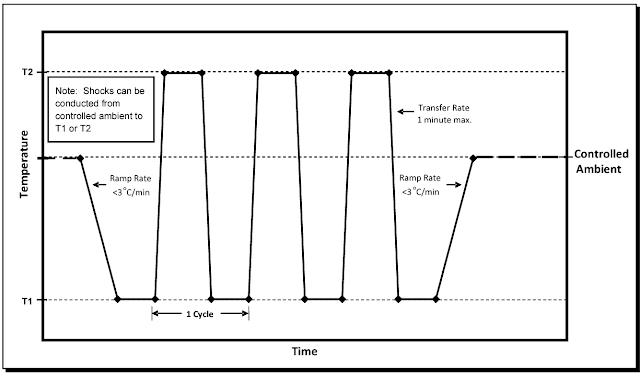
High and low temperature cycling test is a test method to simulate PCB working under different temperature environment.PCB samples are placed in alternating cycles of high and low temperature environments to observe their performance changes and failures.
· High temperatures simulate hot environments, such as outdoors in summer and hot workshops;
· Low temperatures simulate cold environments, like outdoor, refrigerated equipment in winter.
Test Purpose:
Evaluates the stability of materials and structures of PCBs during rapid temperature changes, as well as the reliability of electrical performance, helping to identify problems in advance and providing a basis for product optimisation.
The general temperature cycle is usually in the following temperature sequence as a cycle: room temperature → low temperature → low temperature stay → high temperature → high temperature stay → room temperature
PCB Failure Modes in Testing
Solder Joint Failure
· Thermal expansion coefficient mismatch:PCB solder joints connect components and substrates, different materials have different coefficients of thermal expansion.At high temperatures, the solder expands more than the substrate and components, resulting in thermal stress; at low temperatures and inconsistent contraction, resulting in reverse stress.Repeated cycles cause the stresses to accumulate, ultimately leading to cracks or even breaks in the solder joints, resulting in unstable or interrupted electrical signal transmission.
· Oxidation and corrosion:High temperatures accelerate the oxidation of metal on the surface of the solder joints, generating oxides; humid and low-temperature environments may cause corrosion of the solder joints.Oxidation and corrosion will reduce the conductivity of the solder joints, increasing resistance, affecting the stability and integrity of signal transmission, the number of cycles will increase the problem will be more serious.
Substrate layering
·Separation of resin and reinforcing material: PCB substrate is composed of resin and reinforcing material (such as glass fiber cloth). At high temperature, the resin expands, and the expansion coefficient of the reinforcing material is small. This difference causes the resin to be subjected to tensile stress; at low temperature, the resin shrinks. When the stress exceeds the bonding force, the resin and the reinforcing material will delaminate. After multiple cycles, the delamination range expands, seriously affecting the mechanical and electrical insulation properties of the substrate, and even causing the PCB to be scrapped.
·Amplification of manufacturing process defects: If the substrate material quality is poor or the lamination process is defective during manufacturing, high and low temperature cycles will amplify the problem. For example, the resin is unevenly distributed during lamination, and it is easy to delaminate in the stress concentration area at high temperature.
Component failure
· Chip damage: Chips are sensitive to temperature. High temperatures can cause the chip's operating temperature to exceed the rated range, resulting in performance degradation and accelerated aging. Long-term overheating can cause internal short circuits or open circuits and failure. At low temperatures, chip packaging materials and internal circuits generate stress due to thermal expansion and contraction, which may cause package cracking or internal circuit connection failure.
· Changes in capacitor and resistor performance: High temperatures may cause capacitor electrolytes to dry up and dielectrics to age, resulting in decreased capacitor capacity and increased equivalent series resistance, affecting circuit filtering and energy storage functions. Low temperatures may cause capacitor insulation performance to deteriorate and resistor values to drift, affecting the normal operation of the circuit.
· Copper layer stress concentration: PCB circuit layers are mostly copper foil, and the copper layer expands due to heat at high temperatures, generating stress. If the circuit layout is unreasonable or there are sharp corners, the stress will be concentrated, resulting in tiny cracks. At low temperatures, the cracks may expand, affecting the conductivity of the circuit and even causing a circuit break.
· Mechanical damage accumulation: During high and low temperature cycles, the PCB may be subjected to mechanical vibration or impact, the circuit layer material becomes brittle, and the accumulated damage is prone to cracking. In addition, the additional stress generated by improper installation and fixation will also accelerate the damage of the circuit layer.
How do you deal with these failures?
Optimised design
· Reasonable layout: When designing PCB circuits, avoid sharp corners and narrow lines, use arc transitions and wider lines to reduce stress concentration. At the same time, rationally plan the layout of signal lines and power lines to reduce the impact of electromagnetic interference on temperature changes.
· Choose suitable materials: According to the product use environment and operating temperature range, select substrate materials, solders and components with matching thermal expansion coefficients. For example, in high-temperature environments, select materials with better high-temperature resistance to improve the high-temperature stability of PCBs.
Enhanced manufacturing process control
· Strictly control the lamination process: ensure that the resin is evenly distributed during substrate lamination to avoid defects such as bubbles and delamination. Reasonably control parameters such as lamination temperature, pressure and time to improve the overall strength and stability of the substrate.
· Optimize the welding process: use advanced welding technology to ensure reliable solder joint quality. Control the welding temperature and time to avoid excessive heating to damage components and solder joints. Strictly inspect after welding and deal with problematic solder joints in a timely manner.
Improved environmental adaptation
· Add heat dissipation and moisture-proof measures: In high-temperature environments, heat dissipation devices such as heat sinks and thermal grease can be added to the PCB surface to reduce the operating temperature. In humid environments, use moisture-proof coatings or sealing materials to protect the PCB to prevent solder joint oxidation and components from getting wet.
· Perform stress buffer design: Add elastic buffer materials to the PCB installation and fixing structure to reduce the impact of mechanical stress on the PCB when the temperature changes, such as using rubber gaskets or spring support structures.
In short, high and low temperature cycle testing can reveal the failure mode of PCB in extreme environments. When developing and producing electronic products, service providers should pay attention to this test and take corresponding measures to improve the reliability and safety of PCB, reduce the failure rate, extend product life, and enhance market competitiveness.
Welcome to consult our sales engineer with BOM list and Gerber file

Send your PCB Files or Bom List now
GET IN TOUCHE-mail : Sales@ucreatepcb.com
Office Address : Room 315, Building C, Yunhai Industrial Park, Longgang District, Shenzhen
PCB Factory :Xiangshui River Industrial Zone, Daya Bay, Huizhou. / No. 11, East District, Industrial Park, Suichuan County, Jiangxi Province
SMT Factory : 3/F, Building 28, Chentian Industrial Zone, Xixiang Street, Bao'an District, Shenzhen, China