1. What is Design for Flow (DFM)?
Design for Manufacturability (DFM) involves taking into account factors such as manufacturing processes, costs, and yield during the PCB (Printed Circuit Board) design phase to ensure the design can be produced efficiently and cost-effectively. The goal of DFM is to reduce design defects, improve production efficiency, lower manufacturing costs, and ensure product reliability.
2. The core of DFM testing
The core of DFM testing is to identify and resolve issues that may affect manufacturing in advance during the design phase, avoiding problems that are discovered during the trial production or mass production phase, which may lead to rework or scrap. Its core includes:
-
Manufacturing process compatibility:Ensure that the design meets the process capabilities of the PCB manufacturer (such as line width, spacing, aperture, etc.).
-
Assembling:Consider the feasibility of assembly processes such as SMT (surface mount technology) and DIP (plug-in package).
-
Testability:The design is convenient for ICT (in-circuit testing), AOI (optical inspection) and other testing methods.
-
Cost Optimization:Under the premise of meeting the performance requirements, optimize the design to reduce manufacturing costs.
3. 3. Main contents of DFM testing
DFM testing generally covers the following aspects:
(1) Line and spacing inspection
-
Minimum line width/spacing:Ensure that the line width and spacing meet the PCB manufacturer's process capabilities (such as 4/4mil, 5/5mil, etc.).
-
Differential pair matching:The line width, spacing, and length matching of the differential pairs must comply with the design specifications.
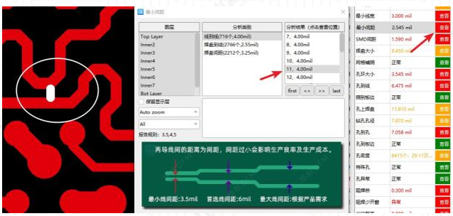
(2) Aperture and via design
-
Via size:The via diameter and pad size must comply with the drilling process (e.g. the minimum via size is 0.2mm).
-
Blind and buried via design:If blind or buried vias are used, make sure the manufacturer supports this process.
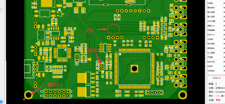
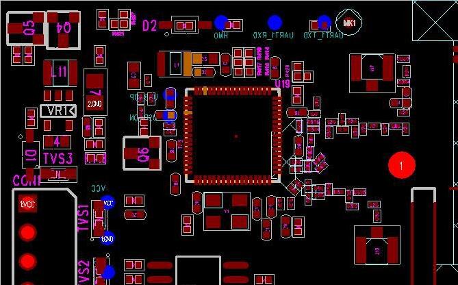
(3) Pad and component layout
-
Pad size:The pad size needs to match the component pins and take the soldering process (such as reflow soldering and wave soldering) into consideration.
-
Component spacing:Avoid placing components too densely, which may affect patching or welding.
(4) Silkscreen and solder mask
-
Silkscreen location:Silkscreen characters cannot cover pads or vias to avoid affecting soldering.
-
Solder mask bridge:Make sure the solder mask does not form short circuits (such as solder mask bridges between SMD pads).
(5) Power and ground planes
-
Power Integrity:Ensure that the power plane is complete to avoid excessive segmentation that may cause noise.
-
Ground plane return path:Optimize ground plane design to reduce signal backflow interference.
4. The significance of DFM inspection
DFM checking plays a vital role in PCB design:
(1) Reduce design rework
-
Identify and resolve manufacturing issues during the design phase, avoiding rework during pilot or mass production, saving time and costs.
(2) Improve manufacturing yield
-
Designs that comply with manufacturing processes can reduce problems such as poor welding, short circuits, open circuits, and improve product yield.
(3) Reduce production costs
-
Optimizing the design (such as reducing the number of vias and optimizing routing) can reduce PCB manufacturing costs.
(4) Reduce time to market
-
Reduce the number of design modifications and trial productions, and speed up product mass production.
5. Conclusion
DFM checking is an essential part of PCB design. It not only improves design quality but also optimizes manufacturing processes, reduces costs, and enhances product reliability. Designers should fully understand the core principles of DFM and conduct rigorous DFM analysis during the design phase to ensure that PCB designs can be manufactured efficiently and cost-effectively.
Recommended tools:
-
Altium Designer(Built-in DFM checking function)
-
Cadence Allegro(DFM rule check)
-
Mentor Graphics Xpedition(DFM analysis tool)
Through reasonable DFM analysis, PCB design teams can significantly improve product competitiveness and ensure the smooth progress of the manufacturing process.
Welcome to consult our sales engineer with BOM list and Gerber file