Categories
Recent Posts
At Ucreate, we've spent over two decades perfecting the art and science of PCB design and manufacturing, handling everything from delicate signal integrity challenges to high-power applications demanding currents exceeding 100 amps. Our ISO 9001:2015 certified facilities and IPC-certified engineering team have witnessed firsthand how proper trace width calculation can transform a problematic design into a market-leading product. Today, we're sharing our expertise to help you understand why this seemingly simple parameter deserves your utmost attention.
The Science Behind the Heat: Understanding Current Flow in Copper Traces
When electric current flows through a copper trace, it encounters resistance – a fundamental property that generates heat according to the power dissipation formula P = I²R. This resistive heating effect becomes exponentially more critical as current increases, making proper trace width calculation not just a design consideration, but a safety imperative.
The resistance of a PCB trace depends on three primary factors: trace width, copper thickness, and trace length. Copper, while an excellent conductor, still presents measurable resistance that increases with temperature. As current flows and generates heat, the copper's resistance rises, creating a feedback loop that can lead to thermal runaway if not properly managed through appropriate trace sizing.
Consider this real-world scenario: A designer creates a motor control board with 2-amp continuous current requirements. Using standard 1 oz/ft² copper (35 micrometers thick) on an external layer, IPC-2221 standards dictate a minimum trace width of 30 mils (0.76mm) for a conservative 10°C temperature rise. However, if this same designer fails to account for motor startup currents that can reach 8-10 amps during stall conditions, those traces become miniature fuses waiting to fail.
Industry Standards: Your Roadmap to Reliable Design
The electronics industry has developed comprehensive standards to guide trace width calculations, with IPC-2221 and IPC-2152 serving as the primary references. These standards, developed through extensive testing by organizations including the Naval Surface Warfare Center, provide the mathematical foundation for determining safe current carrying capacity.
IPC-2221, the classic standard dating back to military specifications from the 1950s-60s, offers conservative estimates that have proven reliable across millions of designs. The standard provides formulas for both external and internal layers:
External Layers: I = 0.048 × ΔT^0.44 × A^0.725
Internal Layers: I = 0.024 × ΔT^0.44 × A^0.725
Where I represents current in amperes, ΔT is the temperature rise above ambient in degrees Celsius, and A is the cross-sectional area in mils² (width × thickness).
IPC-2152, released in 2009, represents modern understanding of PCB thermal dynamics, incorporating factors such as copper planes, environmental conditions, and advanced materials. While more complex to apply, IPC-2152 provides more accurate predictions for contemporary PCB designs, particularly those involving high currents or specialized substrates.
Key High-Current PCB Design Recommendations and Trade-offs
| Design Aspect | Standard Practice (IPC-2221/2152) | High-Current (5A+) Optimization & Trade-Off |
|---|---|---|
| Trace Location | Calculate based on standard layer constants. | Use external layers where possible; size internal traces 20–30% wider for thermal equivalence. |
| Heat Dissipation | Standard FR-4 substrate. | Connect traces directly to large copper planes/pours; use heavy copper (2oz+) for thermal mass. |
| Component Connection | Thermal Reliefs (for manufacturability). | Direct connection to planes for critical current/heat paths, accepting higher assembly risk/cost. |
| Via Strategy | Standard via dimensions. | Use dense via arrays/stitching; optimize for thermal transfer (e.g., 12 mil plated vias) to balance temperatures (ΔT < 5°C). |
| Manufacturing Enhancement | Standard copper/mask. | Apply solder overlay (filleting) to increase current capacity, accepting reduced rework/repairability. |
At Ucreate, our engineering team utilizes both standards, selecting the appropriate methodology based on your specific application requirements. For most commercial and industrial applications, we recommend starting with IPC-2221 conservative estimates, then validating with IPC-2152 for critical high-current designs.
The Hidden Complexity: Why Internal Layers Demand Special Attention
One of the most common and dangerous mistakes in PCB design is treating internal layer traces the same as external layers. Internal traces can require 2-3 times the width of external traces for equivalent current carrying capacity, primarily due to heat dissipation limitations.
External traces benefit from direct air cooling and can dissipate heat through convection and radiation. Internal traces, embedded within the PCB substrate, must rely entirely on conduction through the dielectric material – typically FR-4 with thermal conductivity approximately 1000 times lower than copper. This fundamental difference means that a 10-amp external trace requiring 300 mils (7.62mm) width on an external layer might need 600-700 mils (15-18mm) when routed internally.
Our advanced manufacturing facilities at Ucreate address this challenge through multiple strategies:
Heavy Copper Solutions: When Standard Approaches Aren't Enough
As electronic systems become increasingly power-dense, standard 1-2 oz/ft² copper often proves insufficient for modern high-current applications. Heavy copper PCB technology, utilizing copper thicknesses of 3-10 oz/ft² or more, has become essential for automotive power systems, motor drives, solar inverters, and industrial power converters handling 20-100+ amps.
The relationship between copper weight and current capacity follows predictable patterns, but the manufacturing complexity increases significantly with thickness. Heavy copper PCBs require specialized etching processes, modified lamination cycles, and adjusted design rules for spacing and via sizing.
Our heavy copper PCB division specializes in these demanding applications, offering:
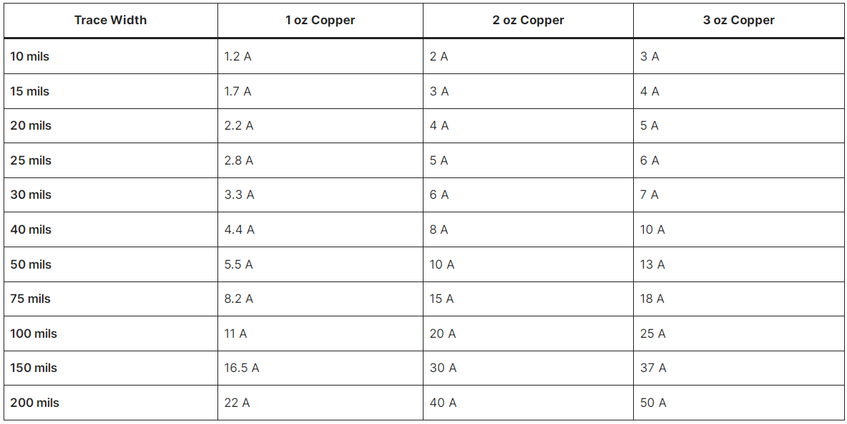
Trace Width vs. Current Tables
Real-World Design Examples: Learning from Success and Failure
Success Story: Automotive LED Driver
A major automotive supplier approached us with a 12V LED driver design requiring 15-amp peak currents for high-beam functionality. Initial designs using standard 1 oz copper and 200-mil traces experienced thermal failures during summer testing in Arizona. Our engineering team redesigned the power distribution using 2 oz copper with 400-mil traces, supplemented by copper pours and thermal vias. The result was a 40°C reduction in operating temperature and successful qualification for automotive production.
Cautionary Tale: Industrial Motor Controller
An industrial equipment manufacturer specified a motor controller with 5-amp continuous current, designing traces accordingly. However, they failed to account for 25-amp inrush currents during motor startup. Field failures occurred within weeks of deployment, with melted traces causing permanent board damage. The redesign, incorporating proper trace width calculations for worst-case currents, increased board cost by 15% but eliminated field failures entirely.
Advanced Considerations: Beyond Basic Width Calculations
While trace width forms the foundation of current carrying capacity, several additional factors require consideration for robust designs:
Our Commitment to Excellence: Why Choose Ucreate
With over 20 years of specialized experience in PCB design and manufacturing, Ucreate has established itself as the partner of choice for engineers facing complex current carrying challenges. Our comprehensive capabilities include:
The Path Forward: Designing for Success
Understanding the relationship between PCB trace width and current rating represents more than academic knowledge – it's the foundation of reliable electronic system design. As systems become more power-dense and reliability requirements intensify, proper trace width calculation becomes increasingly critical to product success.
The investment in proper trace width design pays dividends throughout a product's lifecycle: reduced field failures, improved customer satisfaction, simplified regulatory compliance, and enhanced brand reputation. Conversely, the cost of inadequate design – whether through field failures, redesign cycles, or lost market opportunities – far exceeds the modest effort required for proper analysis.
At Ucreate, we're committed to supporting your success through every stage of the PCB development process. From initial concept through volume production, our team of experts stands ready to ensure your designs meet the most demanding current carrying requirements while maintaining the highest standards of quality and reliability.
Contact our engineering team today to discuss your high-current PCB requirements and discover how our expertise can transform your next project from concept to market success. With Ucreate as your partner, you're not just getting a PCB manufacturer – you're gaining a competitive advantage through engineering excellence and manufacturing precision.
Related Posts:
1.The Role and Addition Method of Process Edge and MARK Point in PCB Design
2.Summary of Reasons Why PCB Board is Seriously Overheated
3.Advantages And Disadvantages Of Thick Copper PCB
4.What Is ENIG Surface Finishing?
5.Halogen-free And Lead-free Processes: Compliance Challenges For Green PCB Manufacturing
Welcome to consult our sales engineer with BOM list and Gerber file

Send your PCB Files or Bom List now
GET IN TOUCHE-mail : Sales@ucreatepcb.com
Office Address : Room 315, Building C, Yunhai Industrial Park, Longgang District, Shenzhen
PCB Factory :Xiangshui River Industrial Zone, Daya Bay, Huizhou. / No. 11, East District, Industrial Park, Suichuan County, Jiangxi Province
SMT Factory : 3/F, Building 28, Chentian Industrial Zone, Xixiang Street, Bao'an District, Shenzhen, China