Categories
Recent Posts
In mass production factories, it's impossible to manually measure every resistor, capacitor, inductor, and even IC circuit on every board using a multimeter. That's why ICT (In-Circuit-Test) automated testing machines were developed. These machines use multiple probes (often called "bed-of-nails") to simultaneously contact all the components on the board that need to be measured. Then, through program control, they measure the characteristics of these electronic components sequentially, primarily in sequence and secondarily in parallel. Typically, testing all the components on a board in this way can be completed in about 1 to 2 minutes, depending on the number of components on the board; the more components, the longer the test takes.
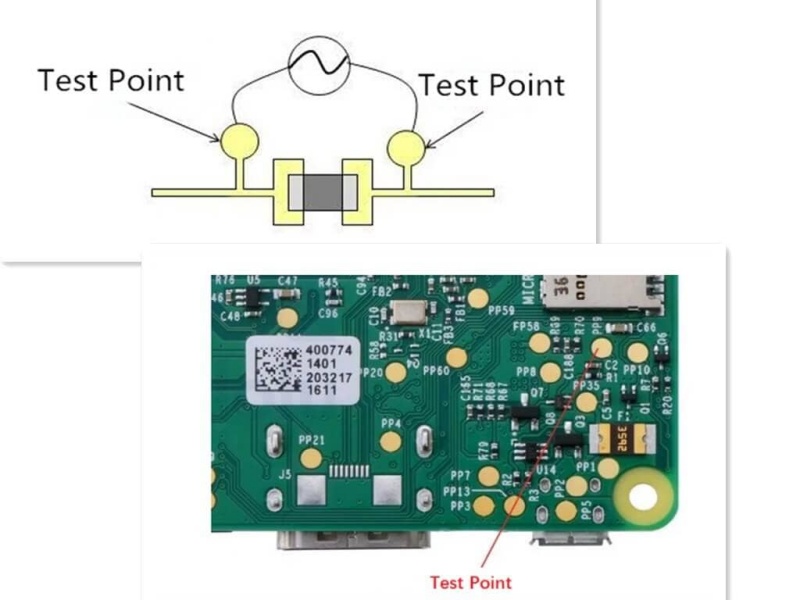
However, if these probes directly contact the electronic components or their solder pads on the board, they could potentially damage some components, leading to the opposite effect. Therefore, clever engineers invented "test points," which are small, circular dots with no solder mask at either end of the component. This allows the test probes to contact these dots without directly touching the electronic component being measured.
In the early days of flexible circuit boards, when traditional through-hole (DIP) connectors were still used, the solder pads were indeed used as test points because they were robust and resistant to pin punctures. However, this often resulted in misjudgments due to poor probe contact. After wave soldering or surface mount technology (SMT), a thin film of solder paste and flux residue typically forms on the surface of the solder. This film has very high impedance, often causing poor probe contact. Therefore, it was common to see test operators on production lines frantically blowing air through the solder or wiping the test areas with alcohol. In fact, wave soldered test points can also experience probe contact problems. After SMT became popular, the situation of test misjudgment was greatly improved, and the application of test points was also given a great responsibility. Because SMT components are usually very fragile and cannot withstand the direct contact pressure of test probes, using test points can prevent the probes from directly contacting the components and their solder feet, which not only protects the components from damage, but also indirectly greatly improves the reliability of the test, because the situation of misjudgment is reduced.
However, with the advancement of technology, circuit board sizes are becoming increasingly smaller. Squeezing so many electronic components onto a small flexible circuit board is already quite challenging. Therefore, the issue of test points occupying circuit board space often creates a tug-of-war between the design and manufacturing ends. Test points are typically circular in shape because probes are also circular, making them easier to manufacture and allowing adjacent probes to be placed closer together, thus increasing the pin density of the probe bed.
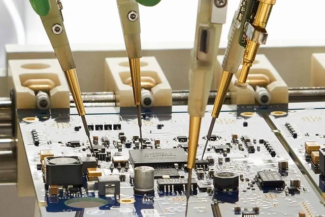
Using a bed of needles for circuit testing has some inherent limitations, such as the minimum diameter of the probes having a certain limit; needles with too small a diameter are prone to breakage and damage.
There are also certain limitations on the distance between needles, because each needle has to come out of a hole, and a flat cable has to be welded to the back of each needle. If the adjacent holes are too small, in addition to the problem of short circuit between the needles, the interference of the flat cable is also a major problem.
There's no way to place probes next to certain tall components. If the probe is too close to a tall component, there's a risk of collision and damage. Additionally, because the components are tall, holes usually need to be drilled in the test fixture's probe bed to avoid them, indirectly making probe placement impossible. It's becoming increasingly difficult to accommodate all the test points for all components on a circuit board.
As flexible circuit boards become smaller and smaller, the question of whether to retain or eliminate the number of test points has been frequently raised. Some methods for reducing test points have emerged, such as Net test, Test Jet, Boundary Scan, and JTAG. Other testing methods are also trying to replace the original bed-of-nails test, such as AOI and X-Ray. However, it seems that none of these tests can completely replace ICT at present.
At Ucreate ELectronic Group, we offer one-stop service from PCB fabricaton,PCB assembly to test services, to ensure that your electronic products meet the highest quality standards. Any quotation, you can contact via email sales@ucreatepcb.com to ger more support.
1. What Is PCB Flying Probe Test?
2.Why the trend of FCT replacing ICT during PCBA test?
3.How to Choose PCB Suppliers?
4.What is Automated Optical Inspection (AOI)?
5.Three Ways to Complete PCB Assembly.
Welcome to consult our sales engineer with BOM list and Gerber file

Send your PCB Files or Bom List now
GET IN TOUCHE-mail : Sales@ucreatepcb.com
Office Address : Room 315, Building C, Yunhai Industrial Park, Longgang District, Shenzhen
PCB Factory :Xiangshui River Industrial Zone, Daya Bay, Huizhou. / No. 11, East District, Industrial Park, Suichuan County, Jiangxi Province
SMT Factory : 3/F, Building 28, Chentian Industrial Zone, Xixiang Street, Bao'an District, Shenzhen, China