Categories
Recent Posts
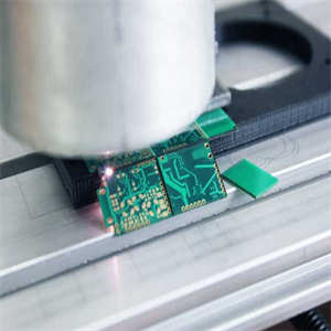
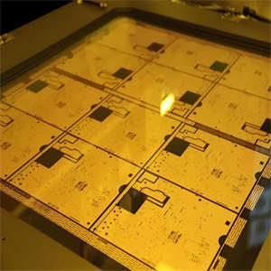
Circuit board shaped processing refers to non-standard (non-rectangular) cutting, drilling or moulding of PCB profiles or internal structures to meet special assembly or functional requirements.Commonlyseen shaped processing include shaped outer contour, stepped slots, blind slots,V-grooves, irregular holes and so on.
The core purpose of special-shaped processing is to adapt to special application scenarios. Specific requirements include:
· Space limitations: For example, flexible circuit boards in wearable devices and folding screen hinges need to conform to complex curved surfaces.
· Functional integration: For example, the sensor module needs to be slotted on the PCB to embed optical components or heat dissipation structures.
· Assembly optimization: For example, by using special-shaped cutting to reduce installation gaps and improve the miniaturization of equipment.
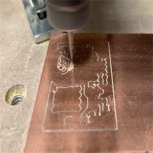
CNC Milling
Laser Cutting
Punching
Plasma/Chemical Etching
· Principle: Use high-speed rotating tools to cut the copper layer and substrate along a preset path.
· Applicable scenarios: high-precision processing of complex outer contours, stepped grooves, V-grooves, etc.
· Advantages: strong flexibility, can be processed into any shape;
· Limitations: Slow processing speed and high cost.
· Principle: Use ultraviolet (UV) or infrared laser to ablate materials to achieve micron-level precision cutting.
· Applicable scenarios: ultra-thin circuit boards (<0.4mm), flexible circuit boards (FPC), tiny holes or curve cutting.
· Advantages: Non-contact processing, no mechanical stress.
· Limitations: Low efficiency in cutting thick plates, and carbonization may occur on the edges.
· Principle: Use customized molds to stamp and form in one go on a hydraulic press or punch press.
· Applicable scenarios: mass production, simple special shapes (such as round holes and square grooves).
· Advantages: fast speed and low cost;
·Limitations: The mold development cycle is long and not suitable for small batches or complex designs.
· Principle: Remove materials through chemical reaction or plasma etching to form a microstructure.
· Applicable scenarios: ultra-fine slots (such as shielding walls of RF circuits).
· Advantages: Suitable for micron-level processing;
· Limitations: Only applicable to specific materials, with high environmental protection requirements.
· Problem: Tool vibration and thermal deformation during milling or laser processing may cause dimensional deviations.
· Solution: Use high-precision CNC equipment (repeat positioning accuracy ±5μm) and real-time temperature compensation technology.
· Problem: Laser cutting or milling may produce burrs and carbonized layers, affecting electrical performance.
· Solution: Optimize cutting parameters (such as feed speed, laser power), and use plasma cleaning or coating repair later
· Problem: Special-shaped designs may result in low substrate utilization and increase production costs.
· Solution: Optimize layout design (such as layout utilization rate ≥ 90%) and choose a cost-effective processing method (such as a combination of stamping + milling).
5. Typical application scenarios of special-shaped processing
· Consumer Electronics:The L-shaped FPC in the mobile phone camera module and the flexible circuit at the hinge of the folding screen.
· Automotive electronics: special-shaped cooling plates in battery packs, sensor-embedded PCBs.
· Medical devices: Ultra-thin, special-shaped circuits and micro-electrode arrays for implantable devices.
Circuit board special-shaped processing is a key link between design innovation and actual production. It is necessary to select the appropriate technical route according to the accuracy requirements, batch size, and cost budget. As electronic products develop towards lighter, thinner, and more multifunctional, the importance of special-shaped processing technology will be further enhanced.
Welcome to consult our sales engineer with BOM list and Gerber file

Send your PCB Files or Bom List now
GET IN TOUCHE-mail : Sales@ucreatepcb.com
Office Address : Room 315, Building C, Yunhai Industrial Park, Longgang District, Shenzhen
PCB Factory :Xiangshui River Industrial Zone, Daya Bay, Huizhou. / No. 11, East District, Industrial Park, Suichuan County, Jiangxi Province
SMT Factory : 3/F, Building 28, Chentian Industrial Zone, Xixiang Street, Bao'an District, Shenzhen, China