Categories
Recent Posts
The ENIG process involves multiple chemical plating processes (such as micro-etching, activation, chemical nickel plating, and immersion gold). If the chemical residues of the previous process (such as micro-etching solution and activation solution) are not thoroughly cleaned, the subsequent plating solution will be contaminated. The contaminated plating solution may cause uneven growth of the nickel layer or introduce impurities, causing local corrosion in subsequent use and forming black areas. In addition, improper control of the pH value, temperature or gold ion concentration of the gold plating solution may also lead to poor adhesion of the gold layer or exposure of the nickel layer, accelerating the oxidation of nickel.
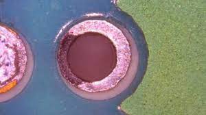
The black disk phenomenon of ENIG usually originates from the corrosion of the nickel layer. The root cause is the uneven distribution of phosphorus content in the nickel plating layer or defects in the plating structure. If the phosphorus content is too low (<7%) during the nickel plating process, the nickel layer is prone to form an easily oxidized crystalline structure, which reacts with oxygen and moisture in the air to form black nickel oxide (NiO/Ni(OH)₂) during subsequent storage or use. In addition, if the porosity of the nickel plating layer is too high (such as the plating layer is too thin or the crystal is rough), the internal copper layer will be exposed, and the copper and nickel will form a galvanic effect (electrochemical corrosion), further accelerating the blackening of the nickel layer.
If the thickness of the immersion gold layer is insufficient (usually 0.05-0.1μm is required) or the gold layer is discontinuous, the nickel layer will be directly exposed to the environment, accelerating oxidation. If the pH value of the gold plating solution is too high (>5.0) or the temperature is too high (>90℃), it may cause partial dissolution of the nickel layer or decrease the adhesion of the gold layer, making the nickel layer more susceptible to corrosion due to contact with air.
- Incomplete cleaning: If the water washing after ENIG is not sufficient, the residual chemical agents (such as the complexing agent in the gold plating solution) may continue to corrode the nickel layer.
- Insufficient drying: If the PCB is not completely dried after cleaning (such as residual moisture), the oxidation of the nickel layer will be accelerated.
- Improper storage environment: If the PCB after ENIG is exposed to a high temperature and high humidity environment (such as humidity>60% RH or temperature>30℃) for a long time, the reaction between the nickel layer and oxygen and moisture will intensify, resulting in the deterioration of the black disk phenomenon.
3. Solution to ENIG black disk phenomenon
√ Process optimization
The black pad phenomenon in the ENIG process is essentially surface oxidation caused by nickel layer corrosion or gold layer failure, which needs to be prevented by optimizing plating solution control, strengthening cleaning and drying, and strict environmental management. The core measures include precise control of nickel/gold plating parameters, improving the density of the plating layer, and avoiding exposure of the nickel layer to the environment, thereby ensuring welding reliability and long-term electrical performance.
Welcome to consult our sales engineer with BOM list and Gerber file

Send your PCB Files or Bom List now
GET IN TOUCHE-mail : Sales@ucreatepcb.com
Office Address : Room 315, Building C, Yunhai Industrial Park, Longgang District, Shenzhen
PCB Factory :Xiangshui River Industrial Zone, Daya Bay, Huizhou. / No. 11, East District, Industrial Park, Suichuan County, Jiangxi Province
SMT Factory : 3/F, Building 28, Chentian Industrial Zone, Xixiang Street, Bao'an District, Shenzhen, China