Categories
Recent Posts

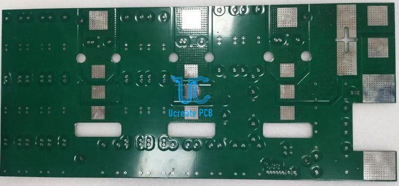
Heavy Copper PCB Manufacturing
Up to 20 oz PCB Manufacturing, rich experience to print solder mask, High quality guarantee for extreme copper PCB.
Send Your Inquiry to Sales@ucreatepcb.com, we will quote you in 2 hours!
Thick copper PCB is divided into single-sided thick copper circuit board, double-sided thick copper circuit board and multi-layer thick copper circuit board. Because of the thicker copper thickness,thick copper circuit board brings a series of processing difficulties to PCB processing. For example, multiple etching is required. , Insufficient glue filling on the pressure plate, cracking of the innerpad of the drilled hole, difficulty in guaranteeing the quality of the hole wall, etc. The minimum aperture of mechanical drilling in pcB processing has dropped from the original 0.4mm to 0.2mm, or even smaller, so the aperture of the metallized hole is getting smaller and smaller. Copper PCB reliability. So, what are the difficulties and precautions in processing thick copper circuit boards?
1. Difficulties in etching
With the increase of copper thickness, due to the difficulty of chemical solution exchange, the amount of side erosion measured will become larger and larger. In order to reduce the large amount of side erosion caused by liquid solution exchange as much as possible, multiple times of rapid etching are required. To solve the problem, as the amount of side erosion increases, it is necessary to compensate for the side erosion by increasing the etching compensation coefficient.
2. Difficulties in lamination
With the increase of copper thickness, the line gap is deeper, and under the same residual copperratio, the required amount of resin filling needs to increase accordingly, so it is necessary to use multiple prepregs to meet the problem of glue filling; due to the need to use resin to the maximum Filling line gaps and other parts, high glue content, and good resin fluidity prepreg is the first choice for thick copper plates. The commonly used prepregs are 1080 and 106. When designing the inner layer, place copper points and copper blocks in the copper-free area or the final milling area to increase the residual copper rate and reduce the pressure of glue filling.
As the copper thicker than the board thickness increases, more heat is required for lamination. The actual heating rate will be slower, and the actual duration of the high temperature section will be shorter, which will lead to insufficient curing of the resin of the prepreg, thereby affecting the reliability of the board; therefore, it is necessary to increase the duration of the lamination high temperature section to ensure The curing effect of the prepreg. If the prepreg is not cured enough, it will cause a large amount of glue removal relative to the core board prepreg, forming a ladder sh
ape, and then the hole copper will break due to the stress.
3. Drilling difficulties
As the copper thickness increases, the thickness of the thick copper PCB also increases. Thick copper plates usually have a plate thickness of more than 2.0mm. Due to the thicker plate thickness and thicker copper thickness during drilling, it is more difficult to manufacture. In this regard, the use of new tools reduces the service life of drill tools, and segmental driling becomes an effective solution for drilling thick copper plates. In addition, the optimization of drilling-related parameters such as feed speed and retract speed has a great influence on the quality of the hole.
For the problem of milling target holes, when drilling holes, the energy of X-RAY gradually decays with the increase of copper thickness, and its penetration ability will reach the upper limit. Therefore, for PCBs with thicker copper thickness, it is impossible to confirm the first board when drilling. In this regard, the deviation confirmation target can be set at different positions on the edge of the board, and the deviation confirmation target line can be milled out on the copper foil accordi
ng to the target position in the data when cutting the material, and the target hole on the copper foil and the inner surface can be cut out during lamination. Layer target holes correspond to production.
Traditional thick copper plates are generally used in fields such as power control and military industry. However, with the rapid promotion of new energy vehicles, the importance of thick copper plates in the field of circuit boards has risen rapidly. It can be expected that the demand for thick copper plates will increase in the near future. There will be explosive growth. But at the same time, the increasingly high requirements of customers have also brought a lot of challenges to PCB man
ufacturers. Leading circuits believes that with the advancement of material technology and PCB manufacturers' technology, many problems will be solved.
If you are looking for a Heavy Copper PCB manufacturer, Ucreate offers complete solutions that you need for your PCB development.
Send Your Inquiry to Sales@ucreatepcb.com, we will quote you in 2 hours!

Send your PCB Files or Bom List now
GET IN TOUCHE-mail : Sales@ucreatepcb.com
Office Address : Room 315, Building C, Yunhai Industrial Park, Longgang District, Shenzhen
PCB Factory :Xiangshui River Industrial Zone, Daya Bay, Huizhou. / No. 11, East District, Industrial Park, Suichuan County, Jiangxi Province
SMT Factory : 3/F, Building 28, Chentian Industrial Zone, Xixiang Street, Bao'an District, Shenzhen, China