Categories
Recent Posts
1. What is a blind or buried via?
A blind or buried via is a through-hole in PCB design used to connect different layers without penetrating the entire board. A blind via connects outer layers to inner layers, whilst a buried via connects only inner layers. Altium Designer supports this type of advanced design.
2. Design Process
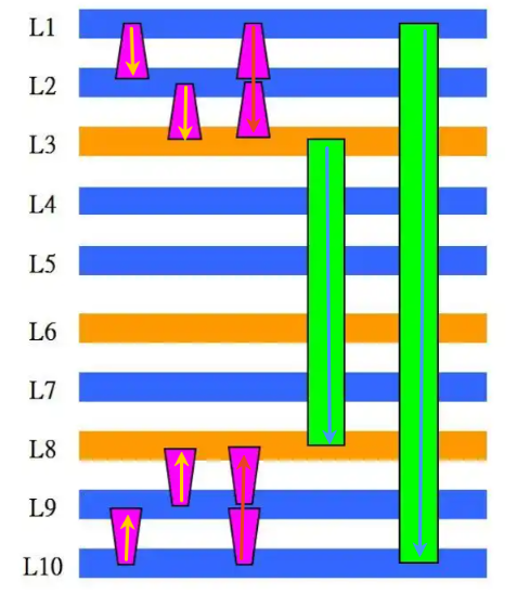
3. Stack-up configuration
Before commencing PCB design, the stack-up structure must be defined, specifying the material and thickness of each layer. Configure this via Design > Layer > Stack Manager, ensuring that sufficient internal layers are included
to support buried via requirements.
4. Defining via types
Set the via type to ‘Blind’ or ‘Buried’ in the PadVia properties. Altum distinguishes between blind vias (Top Layer to Mid-Layer 1) and buried vias (e.g. Mid-Layer 1 to Mid-Layer 2) using the ‘Start Layer’ and ‘End Layer’ properties.
5. Configure the design rules under Design > Rules to set the relevant rules for blind and buried vias:
6. Placing and Verifying Vias
When placing vias using the shortcut keys P+V, select the appropriate layer pair via the Properties panel. Once complete, run a Design Rule Check (DRC) to verify that the blind and buried vias comply with design rules and manufacturing requirements.
7. Manufacturing File Output
When generating Gerber files, tick all relevant layers (including inner layers) in the ‘Output Settings’ section, and annotate the drill positions and depths for blind and buried vias on the ‘DrillDrawing’ layer. Simultaneously,
generate an NC Drill file to enable the manufacturer to identify the via properties.
8. Points to Note
Send your PCB Files or Bom List now
GET IN TOUCHE-mail : Sales@ucreatepcb.com
Office Address : Room 315, Building C, Yunhai Industrial Park, Longgang District, Shenzhen
PCB Factory :Xiangshui River Industrial Zone, Daya Bay, Huizhou. / No. 11, East District, Industrial Park, Suichuan County, Jiangxi Province
SMT Factory : 3/F, Building 28, Chentian Industrial Zone, Xixiang Street, Bao'an District, Shenzhen, China