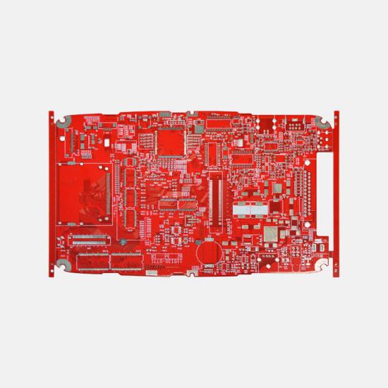
goods stock:
1Layer:
1-32Material:
Fr-4PCB Thickness:
0.8mmCu Thickness:
1.5 OZMin line W/S:
0.1/0.1mmSurface finish:
Immersion goldCertificate:
UL/ISO/IATF16949Application:
Telecom Electronics
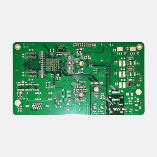
|
Item |
Speci. |
|
Layers |
1~32 |
|
Board thickness |
0.1mm-7.0mm |
|
Material |
FR-4,CEM-1/CEM-3,PI,High Tg,Rogers |
|
Max panel size |
32"×48"(800mm×1200mm) |
|
Min hole size |
0.075mm |
|
Min line width |
3mil(0.075mm) |
|
Surface finish |
OSP,HASL,Imm Gold/Nickel/Ag, Electric gold |
|
Copper thickness |
0.5-7.0OZ |
|
Soldermask |
Green/Yellow/Black/White/Red/Blue |
|
Silkscreen |
Red/Yellow/Black/White |
|
Min PAD |
5mil(0.13mm) |
|
Inter package |
Vacuum |
|
Outer package |
Carton |
|
Outline tolerance |
±0.075mm |
|
Hole tolerance |
PTH:±0.05 NPTH:±0.025 |
|
Certificate |
UL,ISO 9001,ISO14001,IATF16949 |
|
Special request |
Blind hole+Gold finger + BGA |
|
Material Suppilers |
Shengyi, KB, Nanya, ITEQ,etc. |
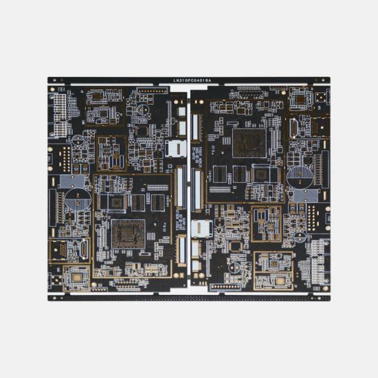
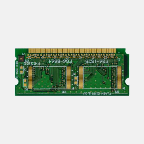
HDI PCB is the short form of high-density interconnect printed circuit board, a kind of printed circuit board manufacturing technology. An HDI PCB is a circuit board with a relatively high circuit density that uses micro-blind and buried “via”—or the copper-plated holes in PCBs—technology. HDI PCB are compact products designed for small-capacity users, as they cost much more than standard PCB.
HDI PCB boards, one of the fastest growing technologies in the PCB industry, HDI PCB contain both the blind via and buried via hole varieties and have a higher circuitry density than traditional circuit boards.
- Guarantee good service and quality from PCB quotation to delivery.
All boards are produced according to IPC-6012 standards and inspected according to IPC-A-600 in the latest version. Our products are widely applied in communications, industrial control, power electronics, medical equipment, security electronics, consumer electronics, LED, etc. More than 90 percent of them were exported to Europe, North America, South America.


Send your PCB Files or Bom List now
GET IN TOUCHE-mail : Sales@ucreatepcb.com
Office Address : Room 315, Building C, Yunhai Industrial Park, Longgang District, Shenzhen
PCB Factory :Xiangshui River Industrial Zone, Daya Bay, Huizhou. / No. 11, East District, Industrial Park, Suichuan County, Jiangxi Province
SMT Factory : 3/F, Building 28, Chentian Industrial Zone, Xixiang Street, Bao'an District, Shenzhen, China