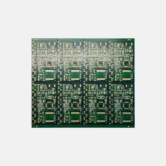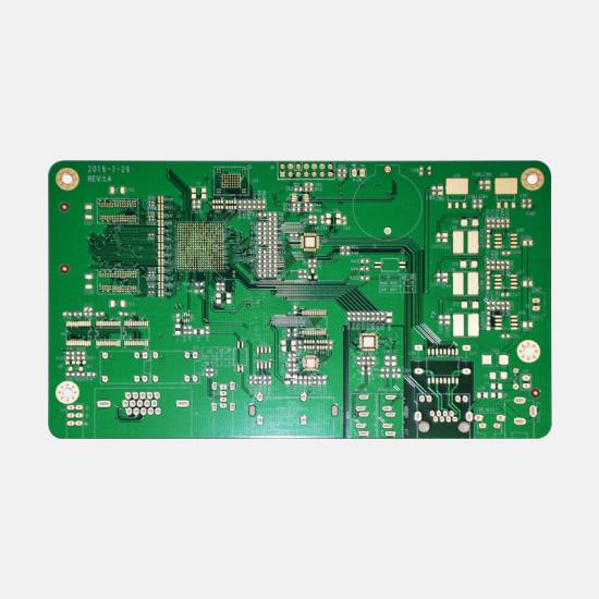
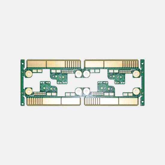
Layer:
2LMaterial:
Fr-4PCB Thickness:
1.2mmCu Thickness:
2.0 OZMin line W/S:
0.1/ 0.1mmSurface finish:
Immersion goldCertificate:
UL/ISO/IATF16949Application:
Industrial Control
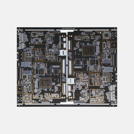
|
Item |
Speci. |
|
Layers |
1~32 |
|
Board thickness |
0.1mm-7.0mm |
|
Material |
FR-4,CEM-1/CEM-3,PI,High Tg,Rogers |
|
Max panel size |
32"×48"(800mm×1200mm) |
|
Min hole size |
0.075mm |
|
Min line width |
3mil(0.075mm) |
|
Surface finish |
OSP,HASL,Imm Gold/Nickel/Ag, Electric gold |
|
Copper thickness |
0.5-7.0OZ |
|
Soldermask |
Green/Yellow/Black/White/Red/Blue |
|
Silkscreen |
Red/Yellow/Black/White |
|
Min PAD |
5mil(0.13mm) |
|
Inter package |
Vacuum |
|
Outer package |
Carton |
|
Outline tolerance |
±0.075mm |
|
Hole tolerance |
PTH:±0.05 NPTH:±0.025 |
|
Certificate |
UL,ISO 9001,ISO14001,IATF16949 |
|
Special request |
Blind hole+Gold finger + BGA |
|
Material Suppilers |
Shengyi, KB, Nanya, ITEQ,etc. |
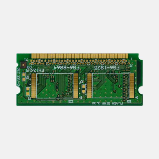
The double-sided PCB is a
common type of printed circuit board. It has wires and components on both the
front and back sides, and the double-sided PCB boards are connected with vias
in the middle. The double-sided printed circuit board has two upper and lower
conductor patterns, and the upper and lower via holes are connected by
expensive perforations. In the processing of printed circuit boards, the hole
walls of your perforated holes are coated with a copper layer to make the upper
and lower layers conductive. Double-sided printed circuit boards are usually
double-sided copper-clad laminates, using screen printing or photo imaging. A
resist pattern is formed on the copper surface, and excess copper foil is
removed by chemical etching to form a conductor pattern.
1. Prepare the circuit
schematic
2. Create a new PCB file and load it into the component package library
3. Planning the circuit board
4. Load the netlist and components
5. Automatic layout of components
6. Layout adjustment
7. Network density analysis
8. Wiring rule setting
9. Automatic wiring
10. Manually adjust the wiring
After the components of the double-layer PCB are drawn in the EDA software, the
wiring sequence is first designed as power line, sensitive line, high frequency
line and low frequency line. It is best to have a separate power supply for the
key lead, a ground return, and the lead is very short, so sometimes a ground
wire is placed close to the signal line on the edge of the key lead to make it form
the smallest working loop.
The signal lines of the double-layer PCB board are the key crystal, crystal oscillator circuit, clock circuit, CPU and other signal lines, which must comply with the principle that the circulating area is as small as possible.
|
PCB Prototype |
Quick Turn PCB |
Single-Sided PCB |
|
Double-Sided PCB |
Multilayer PCB |
Rigid PCB |
|
Flexible PCB |
Rigid-Flex PCB |
LED PCB |
|
Aluminum PCB |
Metal Core PCB |
Thick Copper PCB |
|
HDI PCB |
BGA PCB |
High TG PCB |
|
PCB Stencil |
Impedance Control PCB |
PCB Assembly |
|
High-Frequency PCB |
Bluetooth Circuit Board |
Automotive PCB |
|
USB Circuit Board |
Halogen-Free PCB |
Antenna PCB |


Send your PCB Files or Bom List now
GET IN TOUCHE-mail : Sales@ucreatepcb.com
Office Address : Room 315, Building C, Yunhai Industrial Park, Longgang District, Shenzhen
PCB Factory :Xiangshui River Industrial Zone, Daya Bay, Huizhou. / No. 11, East District, Industrial Park, Suichuan County, Jiangxi Province
SMT Factory : 3/F, Building 28, Chentian Industrial Zone, Xixiang Street, Bao'an District, Shenzhen, China